MCU Design
Current Design
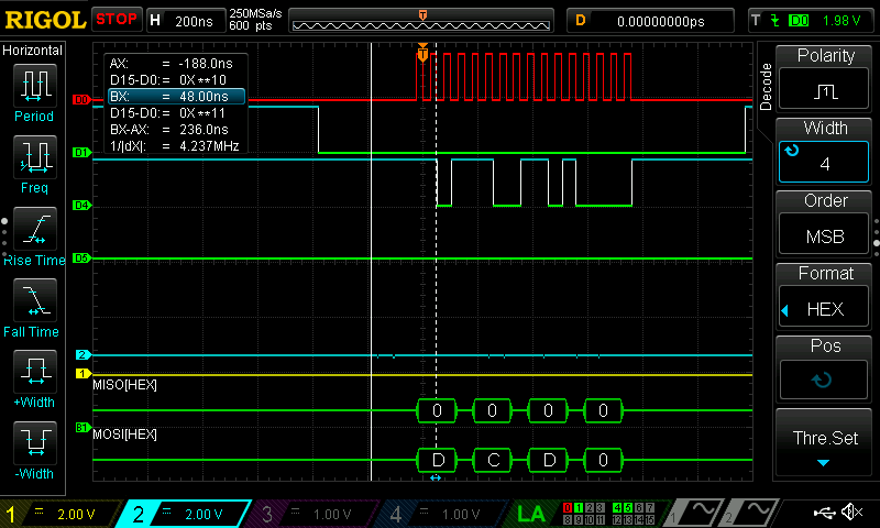
In the project, the MCU was designed to parse and transfer pixel data. A python script grayscaled and downsized a JPEG image so that all the pixel data could fit in the MCU’s SRAM successfully upon runtime at a size of 320x240 pixels. In order for edge detection to be properly applied in the FPGA, the MCU needed to transmist a 3x3 kernal of nibbles. This was perfomed by sending a series of 12-bit packets over the SPI peripheral where each represented one of the image’s columns and within that three consecutive rows of data.

After each kernal is transmitted, the new kernal of data would shift over one column within the image, thus, sending a new 3x3 kernal. Once the the kernal has reached the end of the 240 columns, the matrix would be reset back to the 0th column and shifted down by 1 row.
Original Design
Due to complications in communicating with the ArduCAM Mini 2MP Plus camera module, the project had to downsize heavily on the MCU part. Originally, the I2C peripheral would configure two register banks within the OV2640 camera to alter the resolution and output data format to VGA and RGB565 respectively. After the camera was configured, a SPI peripheral would retrieve pixel data from the module.
To prevent data from being overwritten, a DMA controller faciliated communication between the camera module and the MCU without the need for the processor to intervene. This allowed the processor to focus on other tasks effectively creating a semi-concurrent system. Two DMA channels were used where one was a memory to peripheral transfer system to send clock and fifo-read packets to the camera module while the second channel was a peripheral to memory double buffer reception system. An interrupt was triggered whenever one of the buffers experienced a transaction completed event.
The buffer that triggered the event would then transfer data to the processor to be converted from RGB565 to grayscale data - a critical step to the overall edge detection method. This is where the current system design would be used in choosing specific nibbles to create the 3x3 kernal would be implemented as described above. A third DMA channel, a memory to peripheral transaction, would retrieve the processed data and send it to the FPGA to develop the kernal with a total of three 12-bit data packets.
Camera Module Reflection
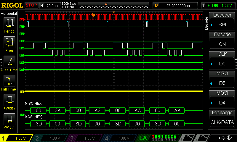
As mentioned before, the camera module would not deliver reliable output data. At times it would deliver valid data, but more often than not, gibberish would be received. This is more likely due to incorrectly configurating the camera module. We manually tried to configure the camera with known register settings with some success. We also reconfigured a public library for a STM32 ArduCAM Mini 2MP Plus camera module congigurations to no avail. On the vendor’s website, we noticed that there was conflicting documentation concerning the SPI peripheral’s clock phase. If there was a major mistake like this, why wouldn’t there be more mistakes within the documentation? This led the team to drop the camera module from the project two days before the official checkoff.

If we were able to redo this project, we would have invested in a better camera with more reliable documentation. It was unfortunate that the team was not able to correctly implement the camera module.